Build your own ByteBlaster
Originally
contributed by Woody Johnson woodyj@dacmail.net
Updated &
Revised by Rune Baeverrud
Please note: Actually - Altera has now officially released the schematics for their ByteBlaster - which you can find by downloading the ByteBlaster datasheet. But I still think you will find the FreeCore version easier to read and use.
![]() June 26,
1997:
June 26,
1997:
The updated schematic is shown below:
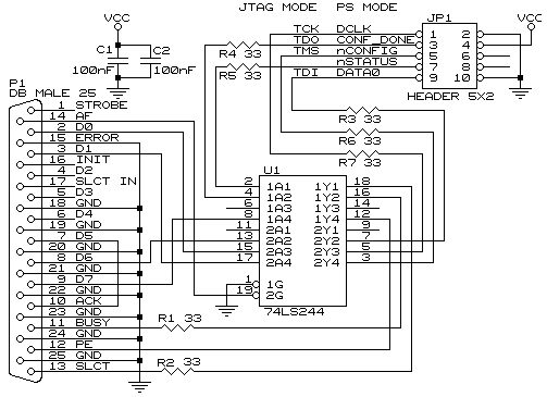
The 74LS244 does not show VCC (pin 20) and GND (pin 10) connected. These pins should be connected to VCC and GND on the target system through JP1. The unused inputs 1A3 and 2A1 on U1 are not terminated in the schematic above, like in the real ByteBlaster. This is not really required as long as the '244 device is a an LS device, because unconnected inputs in LS devices are default HIGH. If you want to terminate these inputs, I suggest you connect them to VCC through a 1kohm resistor (remember - you should never tie LS inputs directly to VCC) to minimize current consumption. If you replace the LS device with an HCT or other CMOS device, you definitely need to terminate these unused inputs. All resistors are 33 ohms.
If you don't have an LS244 laying around, you might try connecting your target system directly to the parallel port on you PC. I suggest you try the following diagram:
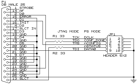
Of course, using this simplified schematic, your success is highly dependent on the driving capability of your parallel port. I recommend using the R1 and R2 series termination resistors for the signals feeding into the parallel port, even if it would probably work well without them. These resistors should be placed as close as possible to the device itself.
 |
To find more ByteBlaster
information, click on the icon on the left to search for 'byteblaster' in the Altera Atlas Solutions Database. |
![]()
Last updated 08 Feb 2001 12:15